Muistihierarkia
Osaamistavoitteet: Tietokonejärjestelmän muistin organisointi hierarkisesti sekä virtuaalimuistin toteutus.
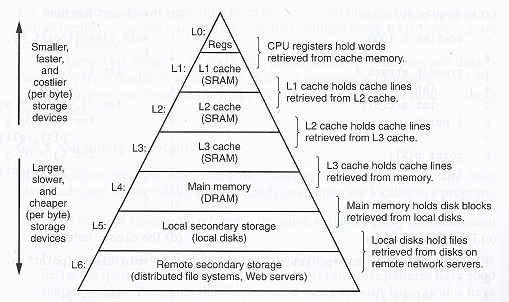
Ensimmäisellä luennolla esittelimme yleisen tietokoneen muistihierarkian. Hierarkian ylimmällä tasolla ovat suorittimen sisäiset muistialueet kuten rekisterit ja välimuistit (ja pino). Mitä lähempänä prosessoria muisti on, sitä nopeampaa se on, mutta sitä on vähemmän ja se on kalliimpaa (per bitti). Pyrkimyksenä on siis säilyttää dataa mahdollisimman lähellä prosessoria suoritustehon maksimoiseksi.
Moderneissa prosessoreissa hierarkian eri tasoilla viiveet jakaantuvat (suunnilleen) seuraavasti:
| Muistin tyyppi | Sijaitsee | Viive (~kellojaksoa) |
| 1. CPUn rekisterit | CPU | 0 |
| 2. TLB-rekisteri | CPU | 0 |
| 3. L1-välimuisti: muistilohkoja (64-bit) | CPU | 4 |
| 4. L2-välimuisti: muistilohkoja (64-bit) | CPU | 10 |
| 5. L3-välimuisti: muistilohkoja (64-bit) | CPU/ulkoinen | 50 |
| 6. Virtuaalimuisti | RAM | 200 |
| 7. I/O-puskurit (laitteiden välimuistit) | RAM | 200 |
| 8. Kiintolevy | Levy-ohjain | 100.000 |
Huomataan, että jopa välimuisteissa on kymmenkertaisia eroja viiveessä. Tämä johtuu siitä, että moderneissa suorittimissa tasojen L1 ja L2 välimuistit ovat yleensä integroitu suorittimeen ja L3 on suorittimesta ulkoinen. Tämä heijastuu myös välimuistien kokoon eli (hieman vanhahtavasti) Eri tasojen välimuistien koko vaihtelee (kymmenistä) kilotavuista muutaman megatavuun (L3). Tyypillisesti sulautetuissa järjestelmissä jäädään alle 1KB kokoisiin välimuisteihin (jolla saadaan mikrokontrollerin hintaa alas).
Paikallisuusperiaate
Kurssilla tähän asti muistiosoitus on ollut suoraa (engl. direct access) tai epäsuoraa (engl. indirect), jossa ohjelmassa on suoraan annettu muistiosoite tai suoritin laskennallisesti muodostaa muistiosoitteen, jolla viitataan keskusmuistiin.
Nyt muistiosoituksia tutkiessa on havaittu, että datan sijoittumista muisteihin hallitsee muistiviittausten paikallisuusperiaate (engl. principle of locality / locality of reference), joka tarkoittaa sitä, että minä tahansa ajanhetkenä ohjelma tarvitsee vain pientä osaa sille varatusta muistista ja johon viittaukset tällöin kohdistuvat. Tätä paikallisuutta tarkastellaan kahdesta näkökulmasta:
- Ajallinen (engl. temporal locality): samoihin muistiosoitteisiin viitataan usein (säännöllisesti)
- Avaruudellinen (engl. spatial locality): muistiosoitukset osuvat usein lähekkäisiin osoitteisiin
-> On siis hyödyllistä on pitää välimuisteissa vain se eniten viitattu osa ohjelmalle varatusta muistista.
Kun ohjelma tekee muistiosoituksen, tarkistetaan siis ensin välimuistihierarkian läpi löytyykö haluttu data välimuisteista. Kun data on löydetty, siirretään muistista aina lohko dataa hierarkian läpi lähemmäksi suoritinta. Samalla, koska hierarkian eri tasoilla on eri määrä muistia, lohkon koko pienenee ja sisältö tarkentuu paikallisuusperiaateiden mukaisesti. Lohkon siirto lähemmäksi suoritinta toteuttaa molemmat ajallisuusperiatteen (tuorein data lähinnä) ja lohkona siirtäminen avaruudellisuusperiaatteen (lähekkäiset osoitteet).
Esimerkki. Silmukkarakenteiden koodi ja data olisi hyödyllistä olla läheisessä välimuistissa kokonaisuudessaan!
Osumasuhde
Muistin organisoimisessa hierarkiaan apuna voidaan käyttää laskennallisia parametreja. Yleinen mittari on osumasuhde (merkitään
h), joka tarkoitaa välimuistiin osuneiden muistiosoitusten suhdetta kaikkiin muistiosoituksiin. Esimerkiksi, osumasuhde
h=95% tarkoittaa, että 95% osoituksista haluttu data oli jo välimuistissa ja 5% pitää hakea alemmilta hierarkian tasoilta. Eli mitä isompi osumasuhde, sen vähemmän hitaita muistiosoituksia on ja sitä nopeampaa ohjelma voidaan suorittaa. Osumasuhteesta
h voidaan laskea keskimääräinen muistioperaation aika (engl. Average Memory Access Time):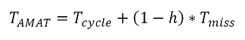
Tässä
Tcycle on kellojakson aika ja Tmiss (maksimi)hakuaika muistista:Esimerkiksi, jos kellojakso on 1ns ja muistin lukuoperaatio 20ns osumasuhteella 95%:
Tamat = 1ns + (1 - 0.95) * 20ns = 2ns
Muistiosoitukset
Aiemmin kerrottiin, että suorittimelta lähtevältä osoiteväylältä luetaan muistiosoite ja sitä vastaava sana haetaan muistista. Tästä käytetään nimitystä lineaarinen muistiosoitus, jossa osoite käsitellään sellaisenaan.
Moderneissa tietokoneissa kuitenkin käytetään muistiosoituksessa apuna sivutusta (engl. paging). Ideana on, että sivuttamalla voidaan osoittaa suurempaa muistialuetta, kuin mihin muistiväylän osoitteen leveys antaisi myöten. Muisti pitää siis jakaa tietyn kokoisiin sivuihin (esim. osoiteväylän leveys tai sitä pienempi). Käyttämättä jääneet tai lisätyt osoitebitit sitten kertovat mistä sivulta dataa haetaan. Nämä bitit saadaan esim. rekisterien ja erityisten osoitemuistipaikkojen avulla ja ne esitetään sivutaulussa (engl. page table). Sivutauluista lisää hetken päästä..
Esimerkki. x86-pohjaisissa tietokoneissa muisti on segmentoitu lohkoihin, joille on annettu tietty käyttötarkoitus. Joukko rekistereitä (CS-GS, kts. kuva johdanto-materiaalissa) varataan muistiosoitteille, jotka kertovat mistä kukin lohko alkaa. Näistä esimerkiksi segmenttiin CS (engl. code segment) sijoitetaan ohjelmakoodi ja segmenttiin DS (engl. data segment) viedään ohjelman data.
Nyt sivutusta hyödyntävä muistiosoite rakentuu kolmesta osasta:
- sivutaulujen sisällysluettelo (sijainti muistissa)
- sivutaulun numero/osoite
- sanan osoite sivulla.
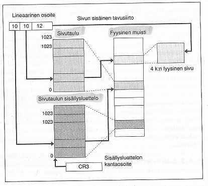
Tässä muistiosoitus menisi niin, että ensin sisällysluettelosta saadaan sivutaulujen osoitteet, sitten haetaan sivutaulu, josta saadaan sivun osoite ja lopuksi sivulta yksittäinen muistipaikka. Kaikki nämä lohkot voivat siis sijaita sikinsokin fyysisessä muistissa.
Kuvassa 32-bittinen (lineaarinen) osoite on jaettu niin, että sivutaulun osoittamiseen sisällysluettelossa on varattu 10 bittiä, sivun sijaintiin taulussa toiset 10 bittiä ja haetun sanan sijaintiin sivulla 12 bittiä. Muistin koko olisi nyt siis
2^32 = 4GB, jossa sivuja on 2^20 = 1048576 kappaletta ja yhden sivun koko 2^12 = 4096B. (Nyt suorittimen ohjauslogiikassa voitaisiin jo nähdä muistiosoitteen osista suoraviivaisesti onko data valmiina välimuistissa, joskun välimuistiin esimerkiksi mahtuu kokonaisia tauluja/lohkoja.)
Välimuistin organisointi
Muistinkäsittelyssä pyrimme siis optimoimaan paikallisuusperiaatteita noudattaen, joka heijastuu muistihierarkian organisointiin. Nyt koska välimuisti on kooltaan aina pienempi kuin alempi taso hierarkiassa, joudutaan välimuistin muistipaikkoja jakamaan hakujen kesken.
Kuvassa muistiosoitteen osat kuvattuna välimuistin organisoinnin näkökulmasta (=oppikirjassa käytetyllä yleisellä esityksellä). Sääntö on että välimuisti organisoidaan joukkoihin (engl. set), joissa kaikissa on valittu määrä lohkoja, jotka koostuvat valitusta määrästä sanoja.
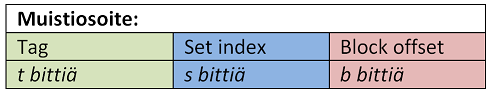
- Tag Lohkon osoite/id, kun joukossa lohkoja on 2^t. Lohko on siis pienin keskusmuistista haettu muistialue.
- Set: Joukko muistilohkoja, kun joukkoja on 2^s
- Block offset (siirtymä, indeksi): Sanan sijainti lohkossa, lohkon koko 2^b sanaa.
Esimerkki. ylläkuvatussa 32-bittisessä muistiosoitteessa Set + Tag voisivat olla 10 + 10 bittiä ja Block offset 12 bittiä.
Tälläinen muistiosoitteen rakenne osoittautuu hyödylliseksi välimuisteja käytettäessä. Seuraavassa esitetään tapoja jakaa välimuistin muistipaikat osoitusten kesken.
Suora kuvaus
Yksinkertaisin osoitustapa on suora kuvaus (engl. direct mapped) jossa muistissa on 2^s joukkoa, joilla jokaisella on käytössään vain yksi välimuistin lohko/muistipaikka. Tällöin Tag-bitit identifioivat mikä lohko välimuistipaikassa milloinkin on.
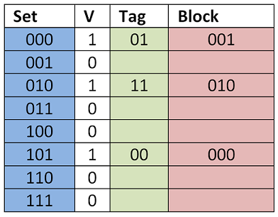
Välimuistin muistipaikan Valid-bitti kertoo, että välimuistin lohko on käytössä. (Muutenhan muistipaikan osoitteessa ja datassa oletusarvot 0 voitaisiin tulkita välimuistiin haetuksi arvoksi..)
Esimerkki. Kahdella tag-bitillä voisimme osoittaa neljää lohkoa. Kun päivitämme välimuistia, Tag-bitit muuttuvat sen mukaan mihin joukkoon osoitamme. Välimuistipaikka pysyy kokoajan samana.
Tag Set Block
--- --- ---
00  000 110
01  000 101
10  000 000
11  000 001
Etuna suorassa kuvauksessa on, ettei joukkoa tarvitse erikseen käydä läpi lohkon löytämiseksi (kts. alla), vaan se saadaan laskettua osoitteesta suoraan. Haittapuolena taas, että muistipaikkoja jaetaan lohkojen kesken, joka voi lisätä muistihakuja ja toisaalta jättää muita välimuistipaikkoja vähäiselle käytölle.
Assosiatiivinen välimuisti
Assosiatiivisessa välimuistissa taas joukolla on useampi välimuistipaikka lohkoille ja lohko voidaan sijoittaa mihin tahansa näistä muistipaikoista.
Yleisesti tällainen välimuisti on E-assosiatiivinen välimuisti (engl. E-way set-assosiative cache). Nimitys välimuistille tulee joukon lohkojen lukumäärän
E perusteella. Kuvassa yllä lohkoja on kaksi per joukko, jolloin E=2 ja puhutaan 2-assosiatiivisestä välimuistista. 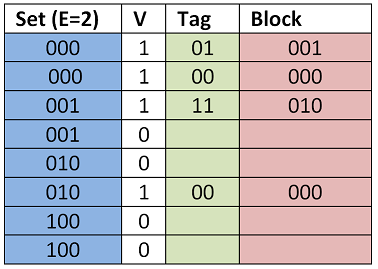
Nyt, datan hakemiseksi välimuistista joudutaan tekemään haku kaikkiin joukon välimuistipaikkoihin, jotta osoitettu lohko löydetään. Oikeissa muistitoteutuksissa lohkoja voi olla esimerkiksi 1024 kappaletta.
Täysin assosiatiivinen välimuisti
Nythän suora kuvaus voidaan käsittää 1-assosiatiivisena välimuistina, koska joukossa mahdollisia muistipaikkoja on vain yksi.
Toinen ääritapaus on täysin assosiatiivinen (engl. fully associative) välimuisti, jossa yksi joukko sisältää kaikki välimuistipaikat. Tälläisessa muistiosoitteessa ei ole Set-bittejä ollenkaan, vaan ovatkin Tag-bittejä. Muistiosoitteen haussa sitten joudutaan pahimmillaan käymään läpin kaikki välimuistin muistipaikat osoitetun lohkon löytämiseksi.
Yksi syy miksi tämä ratkaisu on nykyään olemassa, on että tällaisessa muistissa hakuja voidaan nykyään ohjelmallisesti optimoida hakualgoritmeilla. Tästä lisää hetken päästä virtuaalimuistin yhteydessä.
Välimuistin päivittäminen
Jos haluttua dataa ei löydy välimuistista, tapahtuu cache miss (Suomennos vaikkapa huti..) Nyt data joudutaan hakemaan seuraavan tason välimuistista tai lopulta keskusmuistista.
Muistihausta seuraa välimuistin päivitys, joka voidaan tehdä useilla eri tavoin:
- Suoran kuvauksen välimuistissa osoitettavan lohkon päälle kirjoitetaan aina.
- Assosiatiivisen välimuistin päivitys on työläämpää. Kirjoitettavan välimuistilohkon valinnassa pyritään optimoimaan paikallisuus-periaate. Menetelmiä on seuraavia:
- Vapaa lohko: Jos joukossa on vapaita lohkoja, ne pyritään ensin täyttämään uudella datalla.
- Satunnainen: Valitaan päällekirjoitettava lohko satunnaisesti.
- Least Frequently Used (LFU): Valitaan lohko, johon on viitattu vähiten. Toteutuksessa vaaditaan kirjanpitoa.
- Least Recently Used (LRU): valitaan lohko, johon viittaamisesta on kulunut kauiten aikaa. Vaatii myös kirjanpitoa.
Mutta, ennenkuin uusi data haetaan välimuistiin, täytyy muistipaikassa (mahdollisesti) oleva vanha data kirjoittaa takaisin käyttömuistiin, koska ohjelma on saattanut päivittää sitä. Tätä varten välimuistipaikoissa on useita bittejä, jotka kertovat välimuistipaikan tilasta. Ylläoleva valid-bitti on yksi, mutta bitti voivat kertoa esimerkiksi sisällön muuttumisesta ja datan tuoreudesta. jne.
Muuttuneen datan tallentamiseen välimuistista hierarkian läpi on kaksi tapaa:
- Läpikirjoitus (engl. write-through): Välimuistiin siirrettävä data kirjoitetaan samalla läpi hierarkian kaikkien tasojen.
- Etuna on yksinkertainen toteutus.
- Haittana on merkittävästi pitempi kirjoitusaika. Massamuistiin (esim. kovalevylle) kirjoitus voi olla jopa 100.000 kertaa hitaampaa.. (toki tässä voidaan käyttää massamuistille puskureita.)
- Takaisinkirjoitus (engl. write-back): Data kirjoitetaan muistiin vain kun sitä vastaava välimuistin lohko päivitetään.
- Etuna on, että datan kirjoitus välimuistiin on nopeaa ja usean eri muuttuneen datan päivitys lohkossa vaatii yhden kirjoitusoperaation muistiin.
- Mutta, nyt välimuistin hierarkioiden ja keskusmuistin sisältö voi hetkellisesti poiketa toisistaan!
Toteutuksia
Moderneissa PC-koneissa välimuistin kaksi ylintä tasoa L1- ja L2 ovat yleisesti integroitu suorittimeen ja L3-tason välimuisti taas rakennettu erillisistä piireistä. L3-välimuistin koko on merkittävästi suurempi kuin ylempien tasojen.
Kuvassa Intelin Itanium-prosessorien yleinen välimuistin rakenne.
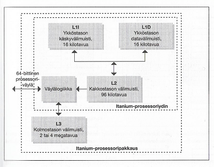
Intelin Xeon-prosessoriarkkitehtuureissa L2-tason välimuistille on oma rinnakkainen nopea muistiväylä järjestelmäväylän rinnalla. Nyt kun L1-taso on integroitu suorittimeen, saadaan myös toisen tason välimuistin toiminta näinollen nopeammaksi.
Virtuaalimuisti
Moderneissa tietokoneissa ohjelmalle ei itseasiassa näy, missä sen käyttämä muisti fyysisesti sijaitsee ja lisäksi muistialue voi olla isompi kuin ohjelmalle jaettu keskusmuistin osa. Tällaista muistiavaruutta kutsutaan virtuaalimuistiksi. Virtuaalimuisti koostuu fyysisestä keskusmuistista ja ulkoisesta massamuistista, esim. kovalevyllä, joka on organisoitu sivutuksella ja välimuisteina niin, että ohjelmalle muistialue näyttää yhtenäiseltä.
Virtuaalimuistin kanssa käytetään virtuaalisia muistiosoitteita, jotka ensin tulkitaan fyysisiksi muistiosoitteiksi ennen muistiosoitusta. Tässä käyttöjärjestelmän palvelut huolehtivat virtuaalimuistin osoitteiden hallinnasta ja suorittavat muistioperaatiot tai prosessorissa voi olla myös MMU-piirejä (engl. Memory Management Unit) osana väyläohjausta, huolehtien muistioperaatioista ja muistiavaruuden hallinnasta.
Etuina saadaan siis:
- Virtuaalimuistilla voidaan tarjota ohjelmille isompi muistialue kuin mitä keskusmuistissa olisi.
- Tietysti virtuaalimuisteissa noudatetaan paikallisuusperiaatteita, mutta huomattavasti isommassa mittakaavassa.
- Keskusmuistia voidaan jakaa ajettavien ohjelmien kesken niiden vaatimien resurssien suhteen.
- Tässä on avuksi, että ohjelmat yleensä tarvitsevat hetkellisesti vain pienen osan koko muistiavaruuttaan.
Muistiosoitukset
Yleisesti virtuaalimuistin osoitus on hidas operaatio, koska data pitää hakea välimuistien kautta, ja pahimmassa tapauksessa massamuistista asti. Nyt välimuistin hallinta voidaan tehdä hardiksen ja laiteohjelmiston yhteistyönä, koska oletuksena haku on hidasta, jona aikana ehditään tehdä monimutkaisiakin optimointioperaatiota!
Virtuaalimuisti jaetaan sivuihin (engl. page), ihan kuten keskusmuistikin. Virtuaalimuistin organisaatio on täysin assosiatiivinen, eli sivu voidaan asettaa minne tahansa keskusmuistissa. Muistiosoitteen kääntäminen virtuaalisesta fyysiseksi tapahtuu osoitemuunnoslogiikan avulla siten että osoitteen ylemmillä biteillä osoitetaan valittuun fyysiseen muistiin.
Esimerkki. Oletetaan
32-bittinen virtuaalinen muistiosoite, jossa lohkolle on varattu 12 bittiä, eli lohkon koko on 2^12B = 4KB. Loput osoitteen 20 bittiä osoittavat muistisivua (ts. set + tag). Tällöin virtuaalimuistin koko olisi 2^20 * 4KB = 4GB. Virtuaalimuistin fyysinen osa taas koostuisi vaikkapa 2^18 * 4KB = 1GB lohkoista muistipiireillä / massamuistissa. 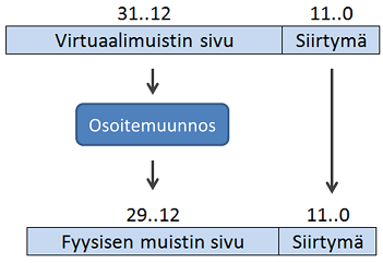
Nopea muistiosoitus
Nopeutta lähtökohtaisesti hitaisiin virtuaalimuistihakuihin saadaan siis, kun osoitettu muisti on valmiina väli/keskusmuistissa. Nyt paikallisuusperiaatteen mukaan, fyysiseksi muistiosoitteeksi käännettyä virtuaalimuistin osoitetta tarvitaan usein, joten käytetyt muistiosoitteet olisi hyvä ottaa valmiiksi talteen välimuistin sivutauluun.
Silti ongelmana on, että huolimatta sivutaulun käyttämisestä, muistiosoituksessa tarvitaan kolme osoitusta muistiin: sivutaulujen sisällysluetteloon, sivutauluun ja fyysiseen muistiin.
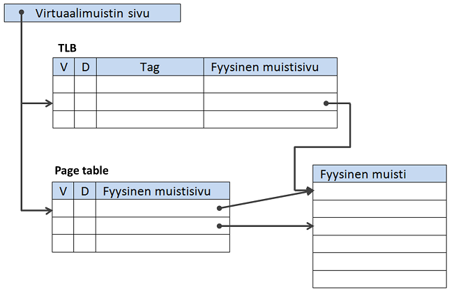
Nyt virtuaalimuistin osoituksia voidaan nopeuttaa tallettamalla jo virtuaalisesta fyysiseksi muunnetut osoitteet rekisteriin tai itseasiassa välimuistiin nimeltä TLB (engl. Translation lookaside buffer). Kun muunnettu osoite löytyy TLB:stä, ei muita välimuistin osoitehakuja tarvitse tehdä.
Koska TLB on välimuisti, täytyy siinäkin olla Valid-bitti kertomassa muistipaikassa olevan datan tila. Lisäksi D-bitti (engl. dirty bit) kertoo onko kyseistä virtuaalimuistin sivua ohjelmassa päivitetty, jolloin se pitäisi päivittää takaisin fyysiseen muistiin, ennenkuin tilalle luetaan uusi sivu.
Muistiosoitteen käännosoperaatio TLB:tä hyväksikäyttäen on seuraava:
- Tarkistetaan löytyykö virtuaalimuistin sivun käännös TLB-rekisteristä
- Jos käännös löytyi, haetaan data annetusta fyysisen muistin osoitteesta
- Jos käännöstä ei löydy TLB:stä, mutta se löytyi sivutaulukosta, riittää että päivitetään TLB haun yhteydessä.
- Jos sivua ei löydy sivutaulukostakaan, joudutaan sivu hakemaan poikkeuksen (page fault) kautta massamuistista.
Osoitteita päivitetään perustuen LRU:hun, jolloin TLB-rekisterissä ja sivutaulukoissa on tilabittejä (engl. reference bit) kirjanpitoa varten kertomassa onko ja milloin sivua on viimeksi luettu.
Virtuaalimuistin takaisinkirjoituksessa käytetään massamuistin hitauden takia write-back-menetelmää, eli kirjoittetava data pidetään puskurissa, joka sitten kirjoitetaan fyysiseen muistiin kerrallaan.
Muistiteknologiat
Nykyisin käytössä on muutama erilainen muistiteknologia, joilla muistihierarkian eri tasot voidaan toteuttaa.
- SRAM (Static random access memory)
- Muistin hakuaika on vakioitu ja on hyvin lähellä kellojakson aikaa.
- Muistisolut (ts. bitit) koostuvat 6-8 transistorin muodostamasta kiikkupiiristä, joka säilyttää bitin arvon niin kauan kuin laitteessa on virtaa.
- DRAM (Dynamic random access memory)
- DRAMssa muistisolun koostuu transistorista ja kondensaattorista. DRAM on siis halvempaa ja muistipiirit tiiviimpiä.
- Bitin arvo säilyy kondensaattorin varauksen avulla, mutta koska varaus purkautuu ajan myötä, pitää soluja virkistää tietyin väliajoin. Virkistys tapahtuu lukemalla bitin arvo puskuriin ja kirjoittamalla se sitten takaisin. Tämä on jokaista bittiä kohden aikaavievää isoissa muisteissa, joten virkistys tapahtuu muistisolu-riveittäin kerrallaan.
- Virkistys itseasiassa nopeuttaa DRAM-muistin käyttöä, koska nyt bitit voidaan lukea puskurista eikä tarvitse erikseen hakea dataa muistista.
- Myös paikallisuuden kannalta tämä on hyödyllistä, kun vierekkäiset bitit voidaan lukea kerralla.
- SDRAM (Syncronous DRAM): Tässä prosessori ja muistipiiri on synkronoitu erillisellä kellolla ja datansiirto voidaan tehdä purskeissa (engl. burst), eli siirtää enemmän dataa kerralla.
- Flash: perustuu EEPROM-teknologiaan
- Muistisoluille on määritelty maksimimäärä kuinka monta kirjoitusta ne kestävät, esimerkiksi 100.000.
- Käytetään usein sulautetuisa järjestelmissä ohjelmamuistina
- Kiintolevy: (ts. kovalevy)
- Hakuaika (engl. seek time): yleensä 3-13ms
- Datan luku- ja kirjoitusaika riippuu myös pyörimisnopeudesta, jne.
- Siirtonopeudet yleensä 100-200MB/s, mutta oman sisäisen välimuistin kanssa jopa 750MB/s (v.2012)
Toteutuksia
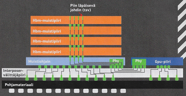
Perinteisesti tietokoneen mikropiirit ovat olleet piirilevyllä rinnakkain, niin että piirilevy kirjaimellisesti on kaksiulotteinen levy. Tästä seurauksena mikropiirien väliset johtimet ovat usein pitkiä, joka osaltaan moderneissa mikropiiriteknologioissa näkyy jo hidastavana tekijänä.
Muistipiireissä uusi HBM-teknologia (engl. High-Bandwidth Memory) kasaakin muistipiirit päällekäin, niin että johtimet kulkevat "pystysuoraan" muistipiirien läpi. Kun piirilevyltä ei viedä pinta-alaa, saavutetaan tällä ratkaisuilla myös leveämpi muistiväylä ja sen myötä voidaan käyttää pienempiä kellotaajuuksia.
Lopuksi
"We are ... forced to recognize the possibility of constructing a hierarchy of memories, each of which has greater capacity than the preceding but which is less quickly accessible."
- Burks, Goldstine & von Neumann (1946)
- Burks, Goldstine & von Neumann (1946)
Vaikka välimuistien ajatus esitettiin jo ensimmäisten modernien tietokoneiden yhteydessä 1940-luvulla, muistinhallinta on kaikenkaikkiaan monimutkainen operaatio moderneissa prosessoreissa monine eri ratkaisuineen jaettuna käyttöjärjestelmän, laiteohjelmiston ja hardiksen kesken.
Anna palautetta
Kommentteja materiaalista?