Käskysykli
Osaamistavoite: Konekielen käskyn suorittaminen sekventiaalisessa prosessorissa.
Kurssilla esitellään y86-64-prosessorista kaksi versiota, joista ensimmäinen, toteuttaa sekventiaalisen käskyn suorituksen. Tämä tarkoittaa sitä, että prosessorissa jokainen käsky suoritetaan kokonaisuudessaan yhden kellojakson aikana. Käskyn suoritus jaetaan ao. mukaisesti pienempiin vaiheisiin prosessorin osajärjestelmissä, jotka suorittavat käskyn peräkkäin saman kellojakson sisällä/aikana. Nyt käskystä riippuen eri osajärjestelmät ovat aktiivisia käskyn suorituksen eri vaiheissa. Perustelu sekventiaaliselle suoritukselle on prosessorin sisäisen toiminnan toteutuksen yksinkertaistuminen, kun käskysykli on sama kaikille käskyille. Tällöin suorittimen ohjauslogiikan toteutukseen tarvitaan vähemmän ohjauslogiikkaa ja osajärjestelmien komponentteja.
Moderneissa suorittimissa tämä on kuitenkin jo hidas tapa suorittaa ohjelmia, kuten tullaan tulevassa materiaalissa näkemään, mutta idea on oleellista ymmärtää ennenkuin siirrytään tehokkaampiin toteutuksiin.
Kaikissa suorittimissa käskyn suoritukseen liittyy rekisteri nimeltä ohjelmalaskuri/PC (engl. program counter / instruction pointer), jossa säilytetystä muistiosoitteesta luetaan suoritettava käsky. Kun käskyn suoritus etenee, tuloksesta riippuen PC-rekisterin muistiosoitetta päivitetään seuraavaksi suoritettavan käskyn osoitteeseen. Kun suoritussekvenssi alkaa taas alusta, PC-rekisterin osoittamasta muistipaikasta haetaan seuraava käsky suoritusta varten.
Käskyn suoritussekvenssi
Käskyn suorittamisessa, käskysyklissä on sekventiaalisessa y86-64:sessa kuusi vaihetta. Käytämme vaiheista (paremman puutteessa) niiden englanninkielisiä nimityksiä:
- Fetch Käsky noudetaan muistista PC-rekisterin osoittamasta paikasta ja se tulkitaan mikro-arkkitehtuurissa, tässä siis kaivetaan esiin operaatiokoodi ja operandi(t).
- Decode Luetaan arvot operandien viittaamista rekistereistä ja asetetaan ne ALU:lle valmiiksi.
- Execute Suoritetaan käskyn operaatiokoodin mukainen aritmeettis-looginen operaatio operandeille / lasketaan muistiosoite muistiviittausta varten / päivitetään pino-osoitin.
- Muistetaan että y86-64-suorittimen ALU osaa vain neljä yksinkertaista operaatiota, mutta itseasiassa nämä riittävät toimivan suorittimen toteutukseen!
- Memory Jos käskyssä on muistiosoitus, arvo luetaan operandina annettuun rekisteriin annetusta muistiosoitteesta tai kirjoitetaan rekisteristä muistiin.
- Write back ALUn operaation tulokset kirjoitetaan tulosrekisteriin.
- PC Update Päivitetään PC-rekisteriin seuraavan käskyn muistiosoite.
Execute-vaihe on pakollinen jokaisessa käskyssä, mutta kaikki käskyt eivät aina suorita kaikkia vaiheita jos ne eivät ole tarpeen. Esimerkiksi, jos käsky ei vaadi muistiosoitusta, niin se vaihe ohitetaan.
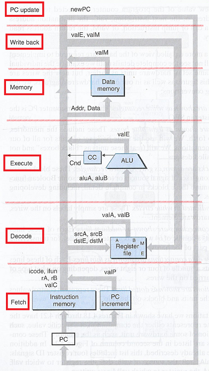
Alla yleiskuvaus y86:sen käskysyklistä. Huomataan, että suorittimen sisäisesti eri vaihden tulokset tallentuvat suorittimen sisäisiin rekistereihin (jotka eivät näy ohjelmoijalle) ja ohjausta kontrolloidaan signaaleina suorittimen eri osajärjestelmien välillä. (Signaali on tässä viesti, jossa voi myös kulkea dataa.)
Tätä käskysykliä sitten prosessorimme jauhaa loputtomiin, ellei poikkeusta tule tai ohjelman suoritus lopu.
Osajärjestelmät
Käydään seuraavaksi osajärjestelmien toimintaa läpi oleellisilta osin.
Kuten kuvasta nähdään niin mikroarkkitehtuurin toteutuksessa käytetään useita eri suorittimen sisäisiä rekistereitä (esim. srcA, dstM, valC, jne..) sekä sekvenssilogiikkaa ohjaavia signaaleja (esim. Cond). Mutta näiden käyttöä ei meidän tarvitse yksityiskohtaisesti käydä läpi ymmärtääksemme käskysyklin toteutus. Toki, tarkempi kuvaus kaikkine detaljeineen löytyy oppikirjasta.
1. Fetch
Ensin käsky noudetaan muistista PC-rekisterin näyttämästä paikasta ja puretaan osiin, jotta käsky suoritetaan sekvenssilogiikan mukaisesti halutusti.
Muistetaan tässä aiemmasta materiaalista konekielen käskyn rakenne:
1. tavu operaatiokoodi: icode (4-bit) + ifun (4-bit)
2. tavu operandit: rekisterikoodit rA (4-bit) ja rB (4-bit)
3-9. tavu: vakioarvo / muistiosoite (8 tavua)
1. tavu operaatiokoodi: icode (4-bit) + ifun (4-bit)
2. tavu operandit: rekisterikoodit rA (4-bit) ja rB (4-bit)
3-9. tavu: vakioarvo / muistiosoite (8 tavua)
Nyt kontrolliosa tulkitsee käskyn seuraavat arvot:
- Operaatiokoodi
icode: käskyryhmä (kts. konekielen luentomateriaali)ifun: operaatiokoodin tarkennus eli suoritettava alifunktio ryhmästä- Operandit, joko
- Rekisteri
rAja/tairB: rekistereitä vastaavat numerokoodit tai merkintä että operandi ei ole rekisteri - Vakioarvo / muistiosoite:
valC - Seuraavan käskyn osoite:
valP, joka on nykyinen PC + tavuina nykyisen käskyn pituus (=hypätään muistissa seuraavan käskyn alkuun) - Jos operaatiokoodi tai muistiosoite ovat virheellisiä, asetetaan poikkeustilat
INStaiADRja ohjelman suoritus päättyy.
2. Decode ja 5. Write-back
Tässä vaiheessa tehdään kaksi toisistaan poikkeavaa toimintoa samalla osajärjestelmällä, koska molemmissa vaiheissa käsitellään rekistereitä:
- Decode-vaiheessa käskyn operandit haetaan/asetetaan ALUlle valmiiksi käskyn suorittamista varten
- Write-back -vaiheessa ALUn operaation tulos viedään tulosrekisteriin
Decode-vaiheessa osajärjestelmässä on kuusi sisäistä rekisteriä, joihin asetetaan luku- ja kirjoitusoperaatioiden kohderekisterien koodit.
- Input
srcA: käskyn ensimmäisen operandin rekisterirA - Input
srcB: käskyn toisen operandin rekisterirB - Output
dstE: käskyn suorituksen tulosrekisterirB - Output
dstM: muistiin kirjoitettava arvorA - Output
valA: rekisteristä noudettu operandi - Output
valB: rekisteristä noudettu operandi
Write back-vaiheessa käskystä riippuen sen tulos sisäisestä rekisteristä
valE kirjoitetaan tulosrekisteriin rB tai muistista haettu arvo valM rekisteriin rA. 3. Execute
Suoritusta varten asetetaan operandien arvot
valA ja valB valmiiksi ALUlle sisäisiin rekistereihin aluA ja aluB. Tällä tavoin ALUn ei tarvitse välittää mitä arvot itseasiassa ovat ja mistä ne haettu, se voi vain suorittaa niille halutun operaation. Suoritettava ALU-operaatio kerrotaan icode:ifun-inputeissa.Jännittävästi y86-64:sen ALU osaa vain neljä operaatiota, mutta näilläkin tosiaan saadaan toimiva tietokone aikaiseksi: yhteenlasku, vähennyslasku, JA-operaatio sekä ERI-operaatio. Huomataan, että konekielen käsky voi loogisesti tarkoittaa jotain muutakin, mutta itseasiassa se vain puretaan joksikin näistä neljästä ALUn sisäisestä operaatiosta!
Itseasiassa, ALUn operaatioista yhteenlasku on käytetyin operaatio, jolla voidaan toteuttaa hyvin erilaisia käskyjä yllättävän yksinkertaisesti, kts. esimerkit materiaalin lopussa..
Kun ALU:n operaatio on suoritettu, operaation tulos tallentuu
valE-rekisteriin. Lisäksi ALU asettaa tilabittien arvot tilarekisteriin CC. 4. Memory
Tässä vaiheessa joko luetaan dataa muistista rekisteriin tai kirjoitetaan rekisteristä dataa muistiin. Operaatio kerrotaan jälleen kerran
icode:ssa. Huomataan periaate muistisijoitukset menevät aina ALUn (ja sen sisäisten) rekisterien kautta eikä operoida suoraan muistiin.Nyt ohjauslogiikka asettaa muistiosoitteen seuraavasti:
- Yleisesti
valE-rekisteristä, joka laskettiin Execute-vaiheessa - Decode-vaiheen
valA-rekisteristä - Fetch-vaiheen
valC-rekisteristä
Kirjoitettava data taas valitaan operaatiokoodin mukaan:
- Yleisesti rekisteristä
valA:sta (Decode-vaiheesta) - Poikkeuksena
call-aliohjelmakutsussavalP:stä (eli seuraavan käskyn osoite) kirjoitetaan pinoon, jotta paluu onnistuu
Muistista haettu data/osoite tallentuu
valM-rekisteriin. 6. PC Update
Viimeisessä vaiheessa tarvitsee enää päivittää
PC-rekisterin arvo, josta seuraava käsky noudetaan uudessa Fetch-vaiheessa. Uusi osoite on joko:
- Yleisesti Fetch-vaiheessa laskettu
valP. - Aliohjelmasta paluu
ret-käskyssä osoite onvalM:ssa, jonne se haettiin pinosta Memory-vaiheessa - Ehdolliset hypyt: operaatiokoodin mukaan joko
valCtaivalP. Nyt siisicodeja tilabitit kertovat vasta tässä vaiheessa suoritetaanko hyppy.
Käskyn suoritusesimerkkejä
Kuvassa esimerkin vuoksi osajärjestelmien toiminta eri tyyppisissä käskyissä. Kuvauksessa käytetään rekisteri- ja muistisiirtoja, joiden syntaksi on seuraava:
R[x]tarkoittaa, että luetaan rekisterin x arvo / kirjoitetaan arvo rekisteriin xM[x]tarkoittaa, että luetaan muistpaikan x arvo / kirjoitetaan arvo muistipaikkaan x- Operaattori
<-tarkoittaa arvon lukemista ja sijoittamista
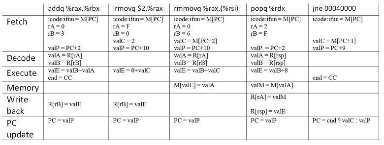
Kuvasta nähdään miten ALU:n operaatiota käytetään eri käskyissä:
addq: Laskutoimitus ja asetetaan tilabititirmovq: Siirto-operaatio yhteenlaskun (nollan kanssa) avulla.rmmovq: Lasketaan muistiosoite, josta luetaan / kirjoitetaan dataa.popq: Haetaan pinosta arvo ja muutetaan pino-osoitetta. Nykyinen muistiosoite ja sanan pituus.jne: Hyppy, jossa tarvitsee lukea tilabitit
Lopuksi
Prosessorin toiminnan ymmärtäminen on avain koko tietokoneen toiminnan ymmärtämiseen. Tässä kappaleessa esittelimme yleisesti sekventiaalisen y86-64:sen toiminnan käskyjen suorituksessa. Sekventiaalisen suorittimen heikkoutena on, ettei siinä käskyn suoritusaikaa voi optimoida, vaan kaikki käskyt suoritetaan hitaimman mukaan. Ts. kellojakso on niin hidas, että kaikki käskyt ehditään suorittaa. Tässä tyypillisesti muistia käyttävät operaatiot ovat hitaimpia. Esimerkiksi von Neumann-arkkitehtuureissa pitäisi tehdä kaksi erillistä muistiosoitusta per käsky. Lisäksi sekventiaalisen prosessorin eri vaiheita toteuttavat osajärjestelmät ovat suurimman osan kellojaksosta tekemättä mitään.
Itseasiassa, sen sijaan että lisättäisiin hardikseen komponentteja tai toiminnallisia digitaalilohkoja parantamaan sekventiaalisen suorittimen toimintaa, voi olla halvempaa tehdä sama operaatio jopa ohjelmallisesti! Ohjelmistolla voi olla myös helpompi hoitaa käskyihin liittyviä erikoistilanteita. Palataan tähän myöhemmässä materiaalissa.
Anna palautetta
Kommentteja materiaalista?