Input / Output
Osaamistavoitteet: I/O-pinnien ohjelmallinen käyttäminen eri tarkoituksiin sulautetussa laitteessa.
Input / Output, eli tuttavallisesti I/O (suom. siirräntä) tarkoittaa informaation siirtämistä tietokoneen komponenttien ja oheislaitteiden välillä. Inputit, ovat komponentin vastaanottamia syötteitä / signaaleja / dataa, kuten näppäimen painallus tai viesti oheislaitteelta. Outputit komponenttien lähettämiä signaaleja tai informaatiota, kuten ohjauskomento oheislaitteelle.
Sulautetun laitteen mikrokontrolleriin itseensä sekä piirikortille on yleensä integroituna valmiita fyysisiä komponentteja ja niiden hallintaan liittyvää logiikkaa I/O:ta varten. Alla listattuna tyypillisimpiä komponentteja, joista osaa tulemme käyttämään kurssilla.
- Painonappeja, liukukytkin, kosketusnäyttö
- LEDejä
- Ajastinpiiri (engl. Timer)
- Analogia-digitaalimuunnin (AD-muunnin, ADC)
- PWM-piiri (Pulssinleveysmodulaatio, engl. Pulse Width Modulation)
- Sarjaliikennepiirejä, kuten UART, SPI ja I2C
- Haihtumatonta muistia, kuten EPROMia
- USB- ja/tai Ethernet-ohjainpiirejä
- LCD-Näyttö
Oheiskomponentit ovat joko digitaalisia tai analogisia. Digitaaliset komponentit ovat usein monimutkaisempia, niissä on erilaisia väyliä ja niiden kanssa pelataan siis bittiarvojen (ts. sovittujen jännitetasojen) avulla.
Analogiset komponentit antavat jännitearvoja, jotka voivat olla mitä vain maatason ja käyttöjännitteen väliltä (esim. 0-3.3V). Esimerkkinä monet yksinkertaiset anturit ilmaisevat mittausarvonsa analogisena jännitteenä. Tietokoneelle tietysti analogiset signaalit on ensin muunnettava digitaaliksi eli numeroarvoiksi, jonka jälkeen niitä voidaan käsitellä numeraalisesti. Tätä toimintoa varten mikrokontrollereissa on valmiiksi integroituna analogi-digitaalimuuntimia, jotka tuottavat jännitteestä (pyöristettyä) numeroarvoa sovitussa tarkkuudessa, esimerkiksi 8-bitin lukualueella (0-255). Picon tapauksessa resoluutio on 12 bittiä, joten arvoja voidaan saada välillä 0–4095.
Nyt ohjelmoijan tehtäväksi jää sitten muuntaa AD-muuntimen antama lukuarvo vastaamaan fyysisen maailman mitattavan suureen arvoa, jonka jälkeen sitä voidaan käsitellä ohjelmassa.
Esimerkkejä tällaisista antureista ovat erilaiset lämpötila- / ilmanpaine- / valaistusvoimakkuus-anturit ja myös mikrofoni. Jos oletetaan lämpötila-anturin mittausalueeksi 0-100C, tällöin ohjelmoijan pitäisi laatia muunnosfunktio AD-muuntimen arvosta (0-255) lämpötilaan (0-100C). Sitten voitaisiin kertoa käyttäjälle laitteen näytöllä, että huoneen lämpötila on esimerkiksi +21C.
Picon HAT-laajennuslevyyn integroidut anturit ovat pääasiassa digitaalisia, joten ADC:n käyttöä ei käsitellä perusmateriaalissa.
Pinni
Okei, katsotaanpa perusteita aluksi. Pinni (myös nasta, engl. pin) tarkoittaa mikropiirin / komponentin fyysistä jalkaa tai liittimen piikkiä. Pinnien / nastojen tarkoitus on komponentin sähköinen ja mekaaninen liittäminen piirilevylle. Piirin jokaisella jalalla / nastalla / pinnillä on tietty käyttötarkoitus. Pinnijärjestys kuvaa mikä tai mitkä ovat pinnien käyttötarkoitukset. Kuten huomataan, joskus yhdellä pinnillä on useitakin eri käyttötarkoituksia riippuen laitteen toiminnallisuuksista. Täten laitteen toiminta on rajoitettua niin että voimme käyttää vain jotain näistä toiminnallisuuksista kerrallaan.
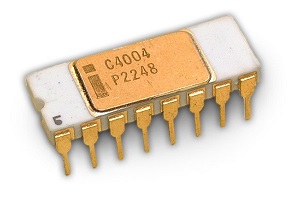
Alla esimerkin vuoksi Intel 4004:n (maailman ensimmäinen kaupallinen mikroprosessori vuodelta 1971) pinnien kuvaus.
Pinnit ja bitit
Ja taas hieman kertausta aiemmasta Bittoperaatiot-luentomateriaalista. Muistetaan, että yleinen periaate on, että ohjelmakoodissa jokaista oheislaitteen ja nyt myös mikrokontrollerin pinniä vastaa yksi bitti, jonka käpistelyyn meillä on C-kielessä ne kuuluisat bittioperaatiot.
- Asettamalla tämä bitti joko loogiseen nollaan tai ykköseen, fyysisen pinnin jännitetaso muuttuu ja näin ohjelmallisesti ohjataan pinniä ja siihen kytkettyä komponenttia / oheislaitetta.
- Vastaavasti luetaan fyysisen pinnin tila (eli jännite) ja sitä vastaava bitti asettuu vastaavaan loogiseen arvoon.
- Loogista ykköstä (engl. High) yleensä vastaa käyttöjännite (tyypillisesti 3.3V tai 5V) tai jännite sovituissa rajoissa. Usein 2.0-2.7V suuremmat arvot tulkitaan ykköseksi.
- Loogista nollaa (engl. Low) vastaa maataso 0V, tai yleensä 0.7V pienempi jännite.
Pinneille annetaan ohjelmoijan (ja elektroniikkasuunnittelijan) työtä helpottamaan niiden toimintaan liittyvä looginen nimi, esimerkiksi
SWCLK, ADC_VREF, USB_VDD, RUN (resetointi) tai GPIO16. Nämä nimet ovat yleensä yhdenmukaisia oheislaitekirjastojen nimien kanssa, eli nimeä vastaa vakio, jonka avulle teemme bittioperaatiot kyseiselle bitille. Esimerkki. Resetoidaan laite nollaamalla
RUN-bitti laitteen ohjausrekisteristä. (Yleensä ohjelmasta ei voi näin suoraan resetoida laitetta, mutta saatiinpahan raflaava esimerkki...) ohjausrekisteri = ohjausrekisteri & ~(1 << RESET);//Nollaa run-bitin rekisterissä
Osa pinneistä on määritelty yleiskäyttöön (engl. General Purpose I/O, GPIO) ja näiden pinnien käyttötarkoituksen voi ohjelmoija vapaasti määritellä, tietysti sen mukaan mitä oheislaitteita niihin kytketään. Loogisesti mikrokontrollereissa GPIO-pinnit on joskus ryhmitelty I/O-porteiksi, niin että esimerkiksi 8 pinniä tulkitaan loogisesti yhdeksi portiksi. Tämä on kätevää, jos laite tarvitsee useita I/O-linjoja, niin niitä voidaan käsitellä loogisesti yhtenä yksikkönä ja ohjata käsitellä kätevästi binäärilukuina. Pico ajattelee kuitenkin kaikkia I/O-pinnejä yksittäin, ellei ohjelmoija itse määrittele loogiset portit haluamilleen pinneille. Tätä ei harjoitustyössä tarvita.
Seuraavissa kuvissa esitetään RP2040-piirin (Raspberry Pi Picon sisällä oleva mikrokontrolleri) pinnijärjestys sekä Raspberry Pi Picon oma pinnijärjestys.
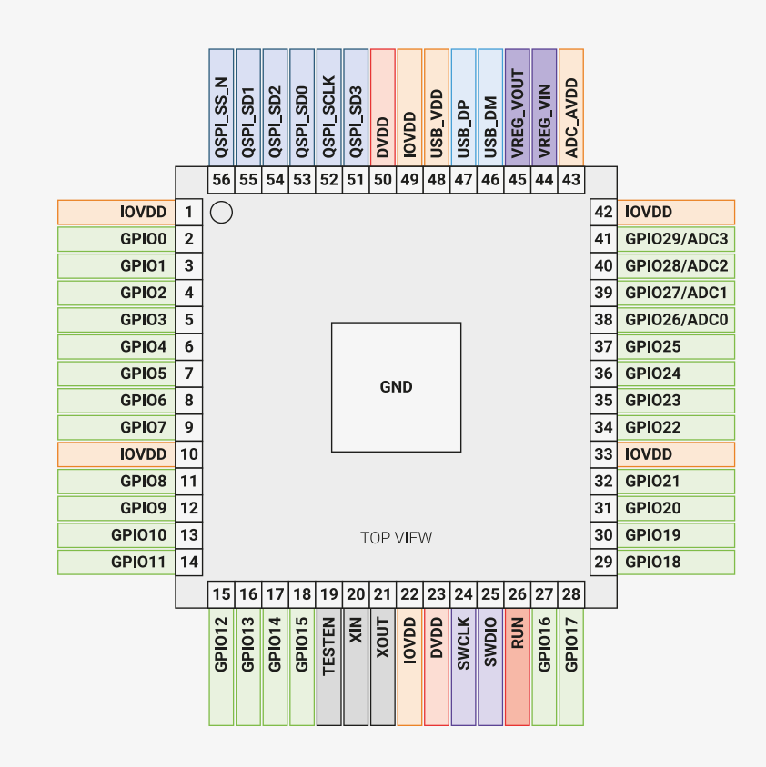
Aiemmin mainittiin, että jotkin pinnit on varattu tiettyihin tarkoituksiin, kun taas toisia voidaan käyttää yleiseen I/O-käyttöön ulkoisten laitteiden liittämiseen. RP2040 on tässä suhteessa joustavampi: se ei määrittele jokaista oheislaitetta kiinteästi tiettyyn pinniin (katso kaikki oheislaitteet |arkkitehtuurikaaviosta). Sen sijaan monet pinnit voidaan konfiguroida eri tehtäviin.
Tämä selittää, miksi Raspberry Pi Picon pinnijaossa useimmilla pinneillä on useita mahdollisia toimintoja. Mutta miten yksi pinni voi palvella eri rooleja? Vastaus on, että RP2040 (ja myös RP2350) mahdollistaa oheislaitteen ”uudelleenohjaamisen” eli kytkemisen johonkin useista vaihtoehtoisista pinneistä. Toisin sanoen voimme päättää, mikä rooli pinnillä on kulloinkin.
Esimerkiksi, oletetaan että haluamme käyttää UART:ia. (Tutustumme UART:iin tarkemmin myöhemmin kurssilla, mutta toistaiseksi riittää tietää, että se tarjoaa kaksisuuntaisen sarjaviestinnän laitteiden välillä käyttäen kahta linjaa: yksi lähettämiseen ja toinen vastaanottamiseen.) Picossa voimme liittää UARTin eri pinnipareihin, kuten pinneihin 4 ja 5, 8 ja 9 tai 20 ja 21.
Muistiinkuvattu I/O
Muistiinkuvattu I/O tarkoitti sitä, että varaamme laitteen keskusmuistista muistipaikkoja (laite)rekistereiksi, jotka on kytketty oheislaitteen pinneihin, ja niiden bittejä käpistelemällä ohjelmassa muuttujien kautta vuorovaikutamme oheislaitteen kanssa. Näiden muistipaikkojen voidaan ajatella muodostavan oheislaitteen vaatimat data-, osoite- ja ohjausväylät, niiltäosin kun moiselle on siinä laitteessa tarvetta:
- Nyt hyödynnetään osoitinmuuttujia, alustamalla ne osoittamaan oheislaitteelle varattuihin muistipaikkoihin. Näiden muistipaikkojen osoitteet sovitaan laitteen suunnitteluvaiheessa ja kun oheislaitteelle tehdään kirjasto, niin ne asetetaan siellä kohdilleen valmiiksi.
- Voimme koodista ohjata oheislaitetta käsittelemällä muistipaikoissa niitä vastaavia bittejä. Sekä asettaa ohjausbittejä että lukea laitteen tila ohjausbiteistä.
- Osana ohjausväylää voi myös olla keskeytyspinni, jonka lähettämä signaali (eli keskeytys) siepataan ohjelmassamme ja siihen reagoidaan halutulla tavalla. No, keskeytyksistä lisää ihan hetken päästä..
- Vastaavasti monimutkaisemmassa laitteessa dataväyläksi valitaan muistipaikka/paikkoja, jotka kytketään oheislaitteen dataväylään (ts. pinneihin) ja näihin saadaan laitteelle välitettyä informaatiota binäärilukuina.
- Joissain monimutkaisemmissa oheislaitteissa, kuten näytöissä, voi olla vielä erillinen osoiteväylä, jonka muistipaikat ovatkin laitteen sisäisiä muistipaikkoja. Jännä.
Ennen kuin tarkastelemme eri tyyppisiä rekistereitä, on tärkeää selventää mahdollinen väärinkäsitys. Kun sanomme, että oheislaitteet ovat muistiosoitteistettuja (memory-mapped), tämä ei tarkoita sitä, että niille annettaisiin RAM-muistia datan tallentamiseen. Tarkoitamme, että oheislaitteet sijaitsevat prosessorin osoitettavassa muistialueessa. Tämä mahdollistaa sen, että prosessori voi lukea ja kirjoittaa niihin samoilla käskyillä kuin RAM-muistiin. Taustalla väylä ja osoite-dekooderi huolehtivat siitä, että kukin muistiosoite ohjataan oikeaan kohteeseen: joko varsinaiseen RAM-muistiin, Flash-muistiin tai oheislaitteeseen. Oheislaitteiden rekisterit eivät ole RAM-soluja, vaan pieniä laitteistoelementtejä, kuten flip-floppeja tai kiikkuja (latches), jotka pitävät sisällään konfiguraatiobittejä tai heijastavat laitteiston tämänhetkistä tilaa.
Rekistereitähän on näin ollen kolmea tyyppiä: osoite-, ohjaus- ja datarekisterit. Oheislaite voi tarjota kaikkiin näihin tyyppeihin useita rekistereitä, mikä vain kombinaatio näistä kolmesta tyypistä laitteen toteutuksesta riippuen on mahdollinen. Picossa esimerkiksi jonkun monimutkaisemman oheislaitteen käyttämiseen voimme tarvita kymmeniä rekistereitä. On siis varsin helpottavaa käyttää oheislaitteen kanssa pelailuun valmiita kirjastoja!
Jokaisesta näistä rekisteristä meidän täytyy siis tietää:
- Yleinen tarkoitus, toiminnallisuudet ja miten niitä käytetään.
- Muistiosoitteet, joissa rekisterit ovat, ja tarjoaako kääntäjäympäristö näitä vastaavat vakiot ja (osoitin)muuttujat valmiiksi.
- Jokaisen rekisterin yksittäisten bittien käyttötarkoitus.
Katsotaan esimerkkinä Raspberry Pi RP2040:n yksi rekisterikuvaus. Tämä rekisteri kuuluu piirissä olevaan jännitesäätimen lohkoon, joka tuottaa DVDD-jännitteen sirun digitaalilogiikan käyttöön.
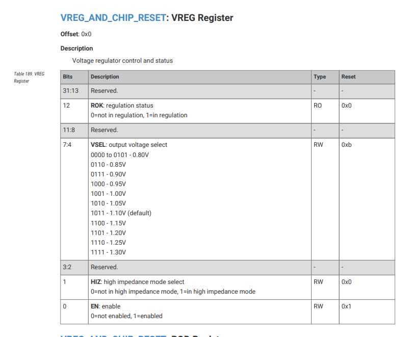
DVDD syöttää prosessorin ytimen ja muut RP2040:n digitaaliset lohkot, ja sen normaali arvo on noin 1,1 V. Tämä on huomattavasti pienempi kuin I/O-pinnoissa käytettävä 3,3 V, koska digitaalilogiikka ei tarvitse yhtä korkeaa jännitettä. Piirin sisäinen regulaattori mahdollistaa sen, että DVDD voidaan generoida sisäisesti IOVDD:stä (3,3 V I/O-jännite) tai jostain muusta 1,8–3,3 V tasoisesta lähteestä.
Kuvasta nähdään, että rekisterin koko on 32 bittiä (
31-0). Osa biteistä on varattu, mutta muutamat kentät sisältävät kiinnostavaa tietoa:Bitit
4-7 muodostavat kentän VSEL, joka valitsee DVDD:n jännitetason.Bitti
1 on HIZ-bitti, joka asettaa säätimen korkeaimpedanssitilaan mahdollistaen ulkoisen regulaattorin käytön.Bitti
0 on ENABLE-bitti, joka kytkee säätimen päälle tai pois (ja näin ollen tekee sirun resetin).Muut bitit ovat varattuja sisäiseen käyttöön.
Jos haluamme muuttaa DVDD:n jännitettä, kirjoitamme VSEL-kenttään. Jos taas haluamme ottaa säätimen pois päältä tai päälle, muutamme HIZ- tai ENABLE-bitin arvoa. Tämä tehdään aivan kuten muidenkin oheislaitteiden kohdalla: lukemalla ja kirjoittamalla rekisteriin sen määritettyä osoitetta käyttäen.
Oletetaan, että haluamme muuttaa jännitteen arvoon 1,15 V (eli kirjoittaa binaariarvon 1100 VSEL-kenttään). Pico SDK tarjoaa
hw_write_masked-apufunktion, jolla voidaan turvallisesti päivittää vain tarvittavat bitit rekisteristä:hw_write_masked(
(io_rw_32 *)(VREG_AND_CHIP_RESET_BASE + VREG_AND_CHIP_RESET_VREG_OFFSET), // VREG-rekisterin osoite
(VREG_AND_CHIP_RESET_VREG_VSEL_1_15 << VREG_AND_CHIP_RESET_VREG_VSEL_LSB), // arvo 1100 siirrettynä oikeaan paikkaan -> 4 bittiä
VREG_AND_CHIP_RESET_VREG_VSEL_BITS // kirjoitusmaski biteille [7:4]
);
Tässä
VREG_AND_CHIP_RESET_BASE + VREG_AND_CHIP_RESET_VREG_OFFSET muodostavat VREG-rekisterin tarkan osoitteen. Symbolinen vakio VREG_AND_CHIP_RESET_VREG_VSEL_1_15 vastaa binääriarvoa 1100, joka valitsee 1,15 V:n ytinjännitteen. Makro VREG_AND_CHIP_RESET_VREG_VSEL_LSB on 4, mikä kertoo, että VSEL-kenttä alkaa bitistä 4, joten arvo täytyy siirtää oikeaan kohtaan. Lopuksi VREG_AND_CHIP_RESET_VREG_VSEL_BITS määrittelee kirjoitusmaskin, joka varmistaa, että vain bitit [7:4] muuttuvat ja muut rekisterin bitit säilyvät koskemattomina.Mutta älä huoli, jos tämä näyttää monimutkaiselta. Sitä se nimittäin on! Yleensä ei tarvitse mennä näin syvälle, sillä SDK:n tarjoama API antaa paljon helpompia tapoja, ilman että sinun tarvitsee tarkistaa rekisterien sisältöjä itse. Meidän tapauksessamme voisimme tehdä saman näin:
#include "hardware/vreg.h"

int main(void){
vreg_set_voltage(VREG_VOLTAGE_1_15); // aseta DVDD arvoon 1,15 V
}
Datakirja
Komponentin tai mikrokontrollerien manuaali, eli datakirja, selittää yksityiskohtaisen pilkuntarkasti kaiken sen sisäisen sekä jokaisen integroidun piirin toiminnan. Datakirja toimii referenssinä laitteistoa ohjelmoitaessa.
Datakirja on tyypillisesti englanninkielinen, vahvasti ammattisanastoon perustuva ja satoja ellei tuhansia sivuja pitkä monimutkaisemmissa laitteissa. Ihan 8-bittisen Arduinon mikrokontrollerinkin datakirja on vajaat 300 sivua pitkä! Eli kun ajatellaan kuinka yksinkertaista pinnien ohjaus on Arduinoilla, sielläkin on takana kymmeniä sivuja datakirjan materiaalia, josta ohjelmoijan ei välttämättä tarvitse tietää mitään. Monimutkaisempien laitteiden datakirjat ovat lähes poikkeuksetta vielä laajempia, esimerkkinä Picon mikrokontrollerin, RP2040:n datakirja. Tässä datakirjassa on 644 sivua!
Onneksi, sen sijaan että kahlaisimme läpi satoja sivuja datakirjoja, kehitysympäristöihin löytyy valmiiksi kirjastoja, funktioita, makroja ja vakioita, joissa on toteutettu valmiiksi oheislaitteiden ohjausta ja korkeamman tason toimintoja varten.
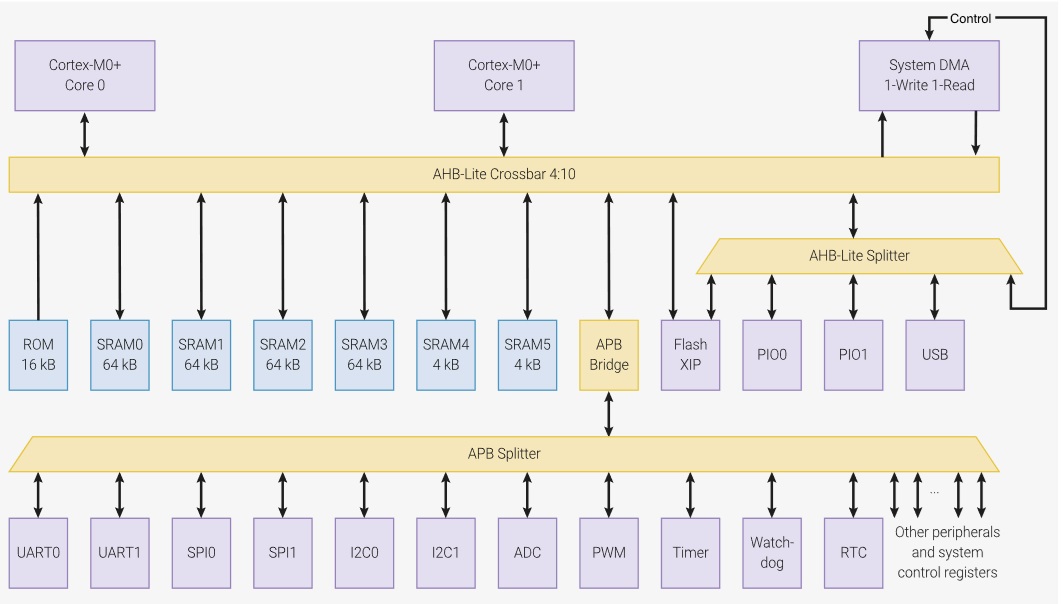
Kurkistus Picoon
Kuvassa lohkokaavio Picon mikrokontrollerin (RP2040) toiminnallisuuksista. Kuten nähdään, Pico on laitteena varsin monimutkainen ja sisältää monta eri toiminnallisuutta. Siihen on integroitu kaksi ARM Cortex M0+-ydintä, joilla on yhteensä käytössään 264 kilotavua SRAM-muistia ohjelmien suoritukseen. Mikrokontrolleri hallitsee useita oheislaitteita, kuten kahta UART-sarjaliikennepiiriä, kellopiiriä ja I2C-väylää. Näistä puhutaankin lisää myöhemmissä materiaaleissa.
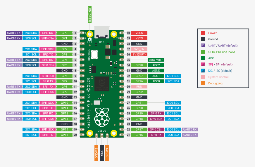
Alla Pico W:n pinnijärjestyksen kuvaus. Pinneille annetaan ohjelmoijan (ja elektroniikkasuunnittelijan) työtä helpottamaan niiden toimintaan liittyvä looginen nimi, esimerkiksi
VSYS tai GPIO6. Suurin osa pinneistä on määritelty yleiskäyttöön (engl. General Purpose I/O, GPIO) ja näiden pinnien käyttötarkoituksen voi ohjelmoija vapaasti määritellä, tietysti sen mukaan mitä oheislaitteita niihin on kytketty. Picossa laitteen suunnitteluvaiheessa myös osalle GPIO-pinneistä on ennalta määritelty mahdollisia käyttötarkoituksia mikrokontrollerin oheislaitteiden käyttöön, ja näitä pinnejä käyttämällä voisimme ohjelmassamme esimerkiksi alustaa sarjaliikennepiirin ja vastaanottaa tai lähettää I2C-dataa.
Picossa sen kirjastot tarjoavat meille valmiita funktiokutsuja näiden pinnien ja niihin kytkettyjen oheislaitteiden käyttöön ohjelmallisesti. Alla on esimerkiksi Picon SDK:n funktiokutsuja
gpio.h-otsikkotiedostosta:void gpio_init(uint gpio);
...
void gpio_deinit(uint gpio);
...
static inline bool gpio_get(uint gpio) {
...
}
I/O-pinnien käyttö
Seuraavaksi perehdymme I/O-pinnien käyttämiseen Picossa koodiesimerkin avulla. Käytössä olevat Picon laajennusalustan vakiot löytyvät kätevästi projektiimme lisätystä otsikkotiedostosta
pins.h.Allaoleva esimerkkimme, kaikessa kauneudessaan käyttää laajennustalustan painonappia on/off-kytkimenä ledille. Eli meidän täytyy tässä määritellä kaksi pinniä ohjelman käyttöön: painonappia vastaava pinni ja lediä vastaava pinni.
Käytämme valmista Pico SDK:n tarjoamaa
gpio-kirjastoa. Koska Picon laajennusalustassa tietyt I/O-pinnit ovat valmiiksi kytkettynä painonappiin ja lediin, saamme niiden määritykset mukaan koodiin otsikkotiedostolla pins.h. Painonapin käyttöönottamiseksi ohjelmassa täytyy tehdä kolme asiaa- Alustetaan nappia ja lediä ohjaavat pinnit
- Tämä tapahtuu
gpio-kirjaston funktiollagpio_init() - Keskeytyksiä käsitellään tarkemmin lähitulevaisuudessa, jolloin niiden ymmärtäminen on helpompaa.
- Laaditaan napinpainalluksen käsittelijäfunktio.
- Alla keskeytysrutiinin käsittelijäfunktio
buttonFxn - ja tietysti
main-funktiossa otetaan nappia vastaava I/O-pinni käyttöön kirjastofunktion avulla - Keskeytyksen käsittelijä asetetaan gpio-kirjaston funktiolla
gpio_set_irq_enabled_with_callback
Tämä esimerkkiohjelma siis, joka kerta kun nappia painetaan, suorittaa funktion
buttonFxn, jossa lediä vastaavan pinnin tila vaihtuu, joka siis näin ohjaa alustan lediä päälle / pois päältä. Esimerkki on purettu osiin alla. #include <FreeRTOS.h>
#include <pico/stdlib.h>
#include <hardware/gpio.h>
#include <task.h>
#include <stdio.h>
#include <inttypes.h>
#include <pins.h>
// Napinpainalluksen keskeytyksen käsittelijäfunktio
void buttonFxn(uint gpio, uint32_t eventMask) {
    // Vaihdetaan led-pinnin tilaa negaatiolla
    uint8_t pinValue = gpio_get(LED1);
    pinValue = !pinValue;
    gpio_put(LED1, pinValue);
}
int main(void) {
stdio_init_all();
// Otetaan pinnit käyttöön ohjelmassa
gpio_init(BUTTON1);
gpio_set_dir(BUTTON1, GPIO_IN);
gpio_init(LED1);
gpio_set_dir(LED1, GPIO_OUT);
// Asetetaan painonappi-pinnille keskeytyksen käsittelijäksi
// funktio buttonFxn
gpio_set_irq_enabled_with_callback(BUTTON1, GPIO_IRQ_EDGE_RISE, true, buttonFxn);
vTaskStartScheduler();
return 0;
}
Puretaanpas ohjelmaesimerkki osiin.
SDK:n muuttujat pinnien käyttöön
Kuten aiemmin mainittu, Picon laajennusalustan SDK tarjoaa meille joukon vakioita
pins.h-kirjastossa. Näitä vakioita käyttämällä voimme käyttää alustan eri oheislaitteita. Tässä tapauksessa haluamme ottaa kirjastosta käyttöömme vakiot BUTTON1 ja LED1.Pinnien alustus
Seuraavaksi alustamme käyttämämme pinnit joko sisääntuloksi (input) tai ulostuloksi (output). Pico SDK:n gpio-kirjasto tarjoaa meille vakioita ja funktioita tämän toteuttamiseen. Vakio
GPIO_IN kertoo kirjaston gpio_set_dir-funktiolle, että haluamme asettaa pinnin sisääntuloksi. Vakio GPIO_OUT taas kertoo samalle funktiolle, että haluamme käyttää pinniä ulostulona. gpio_init(BUTTON0);
gpio_set_dir(BUTTON0, GPIO_IN);
gpio_init(LED1);
gpio_set_dir(LED1, GPIO_OUT);
Tässä siis ensimmäiseksi alustamme pinnin käyttämällä vakioita kirjastosta
pins.h, jotta saamme kerrottua Picolle, mitä pinnejä haluamme ohjelmassa hyödyntää. Kun alustus on tehty, kerromme Picolle, millä tavalla haluamme hyödyntää juuri alustamaamme pinniä. Tässä asetamme pinnin sisään- tai ulostuloksi funktiolla gpio_set_dir. Tämä funktio ottaa argumentteina pinnin, jonka toimintasuunnan haluamme asettaa, sekä vakion, joka määrittelee suunnan sisään- tai ulostuloksi.Pinnikeskeytyksen käsittelijäfunktio
Sisääntuloksi asetetuille pinneille tarvitsemme (yleensä) käsittelijäfunktion, eli siis sen toiminnallisuuden mikä suoritetaan, kun nappia painetaan alas ja tästä aiheutuu keskeytys. Tätä varten ohjelmassamme on toteutettu käsittelijäfunktio
buttonFxn. void buttonFxn(uint gpio, uint32_t eventMask) {
// Vaihdetaan led-pinnin tilaa negaatiolla
uint8_t pinValue = gpio_get(LED1);
pinValue = !pinValue;
gpio_put(LED1, pinValue);
}
Funktio toimii seuraavasti. Ensin luemme ledi-pinnin tilan (päällä "1" / pois päältä "0") funktiolla
gpio_get muuttujaan pinValue. Tämä yleinen funktio tarvitsee argumentiksi pinniä vastaavan vakion LED1, joka siis kertoo sille pinnin, jonka arvon haluamme lukea. Sitten arvolle tehdään negaatio, eli täällä meidän reaalimaailmassa vaihdetaan ledin tilan päälle / pois. Uusi tila asetetaan sitten ledin tilaksi asetusfunktiolla gpio_put. Keskeytys mukaan ohjelmaan
Sitten menemme takaisin
main-funktioon. Alustetut pinnit ovat nyt jo mukana ohjelmassa, mutta meidän pitää vielä asettaa toiselle niistä keskeytyksen käsittelijä, jotta voimme reagoida napin painalluksiin ohjelmassamme. // Painonapille keskeytyksen käsittelijä
gpio_set_irq_enabled_with_callback(BUTTON1, GPIO_IRQ_EDGE_FALL, true, buttonFxn);
RTOS käsittelee taskit ja keskeytyksien käsittelijäfunktiot toisiaan vastaavina toiminnallisuuksina. Keskeytyksistä lisää hetken päästä, mutta nyt kun painonapin tila muuttuu (laskevalla reunalla, koska vakio
GPIO_IRQ_EDGE_FALL) aiheutuu siitä keskeytys. Funktiolla gpio_set_irq_enabled_with_callback asetamme sen funktion joka keskeytyksen seurauksena suoritetaan, ts. on sen käsitteljä. Tässä ohjelmassa siis funktio buttonFxn on tämän keskeytyksen käsittelijä.Huomataan myös, että vakion ja käsittelijäfunktion lisäksi annamme tälle gpio-kirjaston funktiolle muitakin argumentteja. Ensimmäisenä kerromme kirjastolle, mitä pinniä tämä keskeytyksen käsittelijä koskee, tähän asetamme tietysti vakion
BUTTON1, joka tarkoittaa jo aiemmin alustettua nappia. Arvo true, joka annetaan toiseksi viimeisenä argumenttina taas tarkoittaa sitä, että haluamme asettaa keskeytyksen aktiiviseksi heti.Hox! Olisimme tietenkin voineet toteuttaa saman painonapin tilan tarkistuksen superloop-hommina niin, että ikuisessa silmukassa kyseltäisiin joka iteraatiolla painonapin pinnin tilaa, ja jos se olisi muuttunut, tehtäisiin jotain. Taas näitä superloop-hommia, mutta kuten näemme homma hoituu helpommin käsittelijällä.
Analogisen datan tuottaminen: PWM
Mikrokontrollereissa digitaaliset pinnit voivat tuottaa vain kahta arvoa: 0 (low, 0 V) tai 1 (high, yleensä 3,3 V Picossa). Mutta entä jos haluamme himmentää LEDiä, ohjata moottoria tai luoda jotakin, joka näyttää “analogiselta” signaalilta? Tätä varten voimme käyttää pulssinleveysmodulaatiota (PWM). PWM on tekniikka, jossa pinni kytketään nopeasti päälle ja pois, ja päälleoloaika suhteessa koko jaksoon (duty cycle) edustaa keskimääräistä lähtöarvoa.
Aiemmin sanoimme, että jokainen Pico-kortin GPIO-pinni voidaan määrittää käyttämään jotakin laitteistotoimintoa, kuten UART, SPI tai PWM. Raspberry Pi Picossa tähän käytetään
gpio_set_function. Siksi, jos haluamme käyttää PWM:ää pinnillä, meidän on ensin asetettava pinni käyttämään PWM-toimintoa gpio_set_function:lla.RP2040:n sisällä PWM-laitteisto on järjestetty sliceiksi. Niitä on yhteensä kahdeksan, ja jokaisessa slicessa on kaksi kanavaa (A ja B). Voit ajatella slicea perus-PWM-moottorina ja kanavia sen ulostuloina. Jokainen PWM:ää tukeva GPIO-pinni on yhdistetty yhteen näistä kanavista. Tämä tarkoittaa, että jokainen PWM-pinni on jo sisäisesti “kytketty” tiettyyn sliceen. Jotta voimme käyttää PWM:ää oikein, meidän täytyy tietää, mihin sliceen pinni kuuluu. Tiedon voi löytää RP2040:n datasheetistä, mutta käytännössä on paljon helpompaa käyttää SDK:n apufunktiota
pwm_gpio_to_slice_num, joka palauttaa tietyn GPIO-pinnin slice-numeron. Kun slice on tunnistettu, se otetaan käyttöön ja asetetaan pinnille haluttu duty cycle. Jos emme määritä mitään muuta, PWM-laskuri käy oletuksena välillä 0–65535. Siksi myös duty cycle -arvot SDK:ssa annetaan välillä 0–65535: arvo 0 tarkoittaa aina pois, 65535 tarkoittaa aina päällä, ja 32768 on noin 50 % päälläoloaika.Katsotaan yksinkertaista esimerkkiä, jossa säädämme LEDin kirkkautta GPIO-pinniin
LED1 kytkettynä muuttamalla PWM-signaalin duty cyclea.// Konfiguroi GPIO-pinni PWM:lle
gpio_set_function(LED1, GPIO_FUNC_PWM);
// Selvitä, mikä PWM-slice ohjaa tätä pinniä
uint slice_num = pwm_gpio_to_slice_num(LED1);
// Aseta duty cycle (0–65535). Suurempi arvo = kirkkaampi LED.
pwm_set_gpio_level(LED1, 32768); // ~50 % duty cycle
// Ota PWM-slice käyttöön
pwm_set_enabled(slice_num, true);
Edellisessä koodissa:
- Ensin asetamme
LED1toimimaan PWM-ulostulona tavallisen GPIO:n sijaan. - Sen jälkeen selvitämme, mikä PWM-slice kuuluu kyseiselle pinnille. Jokainen pinni kuuluu yhteen sliceen, ja SDK tarjoaa
pwm_gpio_to_slice_numtätä varten. - Tämän jälkeen asetamme duty cyclen
pwm_set_gpio_level:lla. Arvo määrittää maksimin, jonka ajan signaali pysyy korkeana. Sen jälkeen ja uuden jakson alkuun asti signaali on matala. Tässä tapauksessa arvo 32768 on noin 50 % maksimista 65535. Tämä tarkoittaa, että LED on päällä puolet ajasta ja näyttää siksi puolivaloiselta. - Lopuksi otamme slicen käyttöön
pwm_set_enabled:lla, joka käynnistää PWM-laitteiston.
Lopuksi
Muistiinkuvatun I/O:n lisäksi toinen mahdollisuus olisi porttikuvattu I/O, jossa rekistereitä käsitellään erillisten in- ja out-käskyjen avulla. Noh, tätä mekanismia Pico ei käytä.
Mutta hei.. materiaalin perusteella osaat jo tehdä sulautetun ohjelman, joka vilkuttaa laitteen lediä, kun se hoksaa käyttäjän napin painalluksen! Olisko kakkukahvien paikka?